JMS-T2000GC

JMS-T2000GC

High performance gas chromatograph time-of-flight mass spectrometer.

JEM-ARM300F2

JEM-ARM300F2

A new atomic resolution electron microscope has been released! The "GRAND ARM 2" has been upgraded. This new "GRAND ARM 2" enables observations at ultrahigh spatial resolution with highly sensitive analysis over a wide range of accelerating voltages.

JAM-5200 EBM
CRYO ARM 300 II (JEM-3300)

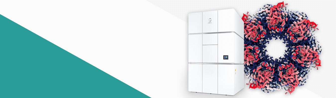
JEM-3300 (CRYO ARM 300 II) Cryo-Electron Microscope

CRYO ARM is an electron microscope for observing biomolecules such as proteins at cryo temperature. The microscope equips a cold field-emission electron gun, an in-column Omega energy filter, a side-entry liquid nitrogen cooling stage, and an automated specimen exchange system. The specimen exchange system can store up to 12 specimens in the specimen exchange chamber.

Electron Microscopy, NMR & Mass Spectometry News

rss

Electron Microscopy News

Our latest blogs on (Scanning) Electron Microscopes, NMR & Mass Spectometry

Release of a new Field-Emission Scanning Electron Microscope: The JSM-7200F

JEOL has released the  JSM-7200F, a multi-purpose FE-SEM combining high-resolution and easy operation.

Scanning electron microscopes have been used in a wide range of fields and for diverse applications. The JSM-7200F utilizes JEOL proprietary in-lens Schottky Plus technology that allows improvement in the resolution at low accelerating voltages (1.6 nm @ 1 kV), and achieves a maximum probe current of 300 nA. The JSM-7200F is a multi-purpose FE-SEM that can satisfy a wide range of needs with both higher resolution and easier operation than conventional instruments.The features include:

  1. High resolution of 1.6 nm at 1 kV, 1.2nm at 30kV.
  2. High-speed analysis: maximum probe current of 300 nA, allowing short acquisition time for EDS, WDS, and EBSD, while maintaining high resolution.
  3. Energy signal differentiation: incorporation of the TTL (through-the-lens) system in the standard configuration enables the use of energy filtering to selectively differentiate the electron energies.
  4. Wide area analysis: the LDF (long depth of field) mode enables applications like wide-area EBSD analysis, without the need to use stage scan (montage).

New Versatile Compact SEM from JEOL


JEOL has released the JSM-IT100, the successor of the very popular and succesful InTouchscope JSM-6010 series. The JSM-IT100 is a simple-to-use versatile, research-grade SEM with a compact ergonomic design.

The JSM-IT100 is very easy to use, due to the very intuitive user interface and has a formidable price-performance ratio. This compact SEM is a versatile workhorse SEM that can be configured to meet individual lab requirements. It offers high resolution imaging, and offers a range of acceleration voltages at both high and low vacuum modes.

With the JSM-IT100, it is simple to quickly obtain high quality images using both Secondary Electron and Backscatter Imaging. The embedded JEOL EDS system with silicon drift detector technology now includes Spectral Mapping, Multi-Point Analysis, Automatic Drift Compensation, Partial area, Line Scan, and Mapping Filter functions.

JEOL's popular InTouchScope series includes the NeoScope benchtop SEM with selectable HV/LV and the JSM-IT300LV with advanced analytical capabilities and imaging of large, intact samples.


New TEM for Naturalis

The Naturalis Biodiversity Center, a research institute and natural history museum in Leiden, has recently acquired the state-of-the-art JEM-1400Plus Transmission Electron Microscope (TEM) from JEOL.

 “Thanks to this TEM we are able to study the biodiversity of plants and species in the smallest details.” According to Kees van den Berg, Senior Analyst at Naturalis. “For the acquisition of the new 120kV TEM the JEM-1400Plus from JEOL was selected because of its performance, ease-of-use and proven stability of the system. The excellent service track record of JEOL also played an important role in the evaluation."

"We used to have a JEOL JEM-1010 from 1992. Even though it was still working well, it no longer fit in our new organization structure where digitalization of our collection and data has become a priority. Additionally, the new TEM is also fully compatible with our Windows 7 based network. The JEM-1010 will go to a new owner who will certainly  benefit from the microscope for years to come."

Since the introduction of the JEM-1400 in 2007 and the JEM-1400Plus in 2012, already more than 600 microscopes of this type have been installed worldwide. The strength of this system lies in the flexibility of the system to be able to work in a great variety of research fields, for example: Biological sections, polymers, nanomaterials and asbestos analysis, all in both room temperature and under cryo conditions. 


JEM-ARM300F: The Ultimate Atomic Resolution Transmission Electron Microscope

Transmission electron microscopy (TEM) has long been a tool essential for micro structure evaluation in the field of materials development.
However, as the fine structures of advanced materials are being designed at the nano level or atomic level, the synthetic process for such materials increasingly requires imaging and analysis at higher resolution.

To meet this demand, JEOL has focused on development of a transmission electron microscope incorporating spherical aberration correctors to exceed the current resolution boundary.
In 2009, JEOL announced the JEM-ARM200F, a 200 kV atomic resolution analytical transmission electron microscope featuring spherical aberration correctors, which achieved a resolution of 80 pm (scanning transmission (STEM) image) as the first ever commercial electron microscope.  To achieve the atomic level resolution, the JEM-ARM200F incorporates various capabilities to ensure highly stable operation.  With over 100 units of the ARM200F currently in operation worldwide, many researchers have become familiar with atomic level imaging and analysis.

JEM-ARM300F
Meanwhile, as aberration correctors are widely used, various new requirements for transmission electron microscopy are emerging, in addition to higher resolution, including higher analytical sensitivity, in-situ imaging, flexible accelerating voltage control, and ease of operation for aberration correction.

Thus, JEOL developed the JEM-ARM300F, a 300 kV atomic resolution transmission electron microscope featuring JEOL's own aberration correctors as an enhanced model of the JEM-ARM200F.
Nicknamed GRAND ARM, the JEM-ARM300F, incorporates JEOL's propriety dodecapole correctors, successfully increasing the resolution level to 63 pm (STEM resolution).
The GRAND ARM can be configured for ultra high resolution imaging or analytical applications for high sensitivity and in-situ analysis according to the user's needs.


The system is primarily intended for public and private research institutes and semiconductor manufacturers.

Main Features

  1. Ultra high resolution imaging
    Achieves a resolution of 63 pm in the scanning transmission electron microscope image (STEM) mode at an accelerating voltage of 300 kV, using JEOL's own spherical aberration corrector for the illumination system.
  2. High performance cold-cathode field-emission electron gun featuring high brightness and low energy dispersion
    Incorporates a new high performance cold cathode electron gun as standard; the high brightness beam with minimum chromatic aberration allows for high resolution imaging and analysis.
  3. Wide accelerating voltage range
    Supports accelerating voltage levels of 300 kV and 80 kV as standard; other accelerating voltage levels are optionally available as needed.
  4. Aberration corrector integrated with microscope base unit
    Incorporates JEOL's proprietary spherical aberration correctors in the image forming system (TEM aberration corrector) and in the illumination system (STEM spherical aberration corrector).
  5. Aberration corrector control system
    Uses the JEOL COSMO (JEOL Corrector System Module) system for auto control of the aberration correctors.
  6. Two types of objective lens pole piece
    Two types of objective lens polepiece are available to meet a wide range of users' applications.
  7. Vacuum system featuring dry pre-evacuation and high vacuum
    The vacuum system features a pre-evacuation system incorporating a turbo molecular pump as standard and an enhanced column evacuation system, achieving higher vacuum while minimizing contamination and damage in atomic level imaging and analysis.
  8. Stable column/console, specimen stage, and electrical system
    The column, 330 mm in diameter, features a higher level of mechanical rigidity.  The microscope base unit is also designed to enhance its mechanical/electrical stability and resistance to environment, fully utilizing the stabilizing technologies developed for the JEM-ARM200F.
  9. A complete line of signal detectors
    A complete line of signal detectors are available, including EDS (energy dispersive X-ray spectrometer) up to 100 mm2and EELS (electron energy loss spectrometer), backscattered electron detectors, and up to 4 STEM detectors.  The microscope also supports simultaneous observation of high angle annular dark field image, low angle annular dark field image, annular bright field image, and bright field image.

Main Specifications

Accelerating voltage Maximum 300 kV
TEM lattice resolution 0.05 nm(with spherical aberration corrector for image forming system)
STEM resolution 0.063 nm(spherical aberration corrector for illumination system)


Specify Alternate Text

JCM-6000 ”NeoScope™”, A New Desktop Scanning Electron Microscope

JEOL's JCM-5000 NeoScope, since it was announced, has been widely used by electronics manufacturers, including semiconductor device makers, as a desktop scanning electron microscope featuring the same ease of operation as optical microscopes for inspection of the products developed and processed by micro technologies. The new JCM-6000 "NeoScopeTM," is a touch panel controlled, multi functional desktop scanning microscope that answers the increasingly diversified needs among users worldwide. Nikon has joined JEOL to sell the Neoscope.

Features

1) Simple operation

  • Easy touch panel operation
  • A complete range of automated functions (auto focus, auto stigmator, auto contrast/brightness)
  • Easy, dependable auto gun alignment (filament centering)

2) Enhanced low vacuum capability

  • Enhanced quality of backscattered electron images
  • Easy observation of non conductive samples in the direct low vacuum mode
  • Only 2 minutes 30 seconds from sample loading to imaging

3) New capabilities for imaging

  • Secondary electron imaging and backscattered electron imaging supported at high vacuum
  • Dual frame imaging to facilitate comparison of live and retrieved images
  • A wide magnification range from the lowest 10x for wide area of view up to 60,000x

4) A complete line of optional accessories

  • Energy dispersive X-ray spectrometer
  • Tilt/rotation motor drive specimen holder

    *Both options are retrofittable

5) Compact, light, and energy saving

  • Base unit: 330mm (W) x 490mm (D) x 430mm (H); 50 kg
  • Utility: Single phase 100 V to 240 V, 50/60 Hz, 700 to 960 VA

JPS-9030: The XPS for high-speed, high-precision depth profiling

In recent years, there has been a growing demand to perform high quality surface analysis quickly, easily and reproducibly on any kind of sample for any level user. The JPS-9030 is equipped with a newly-designed user interface that further improves operability and also debuts a sophisticated, new modern and sleek exterior design.

Main Features

  1. Depth profiling optimized for the application
    The newly-developed Kaufman-type etching ion source provides etching rates from 1 nm/min to 100 nm/min (SiO2equivalent), and allows a wide range of settings. It is capable of depth profiles suitable for any application, from measurements demanding precision to processes that require speed. The mounting of the Kaufman-type etching ion source to the specimen exchange chamber facilitates prevention of  contamination of the measurement chamber.
  2. Newly-developed software provides even greater ease-of-use
    SpecSurf Ver. 2.0 now incorporates a ribbon-style GUI, offering a user-friendly environment in which all operations can be performed with the mouse. With JEOL’s own automatic qualitative analysis function, it is possible to sequentially perform qualitative, quantitative and chemical state analyses for multiple acquisition points.
  3. Ultra-high surface sensitivity
    The JPS-9030 supports techniques like Angle-Resolved XPS (ARXPS) and Total Reflection XPS (TRXPS), and is capable ultra-high sensitive analysis of the top surfaces of 1 nm (standard measurement method 6 nm or more).
  4. A wealth of options
    • Monochromatic X-ray sources
    • Argon gas cluster ion source suitable for organic samples
    • Infra-red heating system capable of temperatures of 1,000°C or higher
    • Transfer vessel to protect specimens from exposure to the atmosphere

Main Specifications

Intensity
(MgKα, 300W equivalent)
1,000,000 cps or more (at Ag3d5/2FWHM is 1.0 eV)
X-ray source Mg/Al twin anode
Input-lens system Cylindrical electrostatic lens
Energy analyzer Electrostatic hemispherical analyzer
Energy sweep method Constant Analyzer Energy and Constant Retarding Ratio
Detector multichannel plate
Ion gun Kaufman type ion gun
Base pressure 7 × 10⁻⁸Pa or better
Bake-out system Built-in heater, automatic control
JPS-9030

JEM-2100Plus: A new 200kV Transmission Electron Microscope

The JEM-2100Plus is a multi purpose transmission electron microscope for micro structure evaluation, which combines the proven JEM-2100 optic system with an advanced control system for enhanced ease of operation. Achieving superior performance through very user friendly intuitive operation, the JEM-2100Plus provides solutions to a wide range of applications from materials science to medical/biological studies.

Main Features


Designed to ease of operation

  1. 64 bit Windows® compatible control software, TEM Center, is an intuitive user interface designed to maximize ease of operation.
  2. A complete range of automated functions
    The JEM-2100Plus comes with a complete range of automated functions, including auto focus, auto contrast/brightness, auto exposure, auto montage, drift compensation, and stage navigation.
  3. Advanced integration
    The TEM Center allows the user to control optional accessories such as high resolution camera and scanning image (BF/DF) observation device through intuitive user-system interaction.
  4. Image view/edit software
    Viewer software supports off-line image viewing and editing.

Notices:Windows is a registered trademark of Microsoft Corporation in the United States and other countries.

Main Specifications

Maximum accelerating voltage 200kV
Guaranteed resolution 0.14 nm(TEM lattice image)
Magnification x30 to x800,000
The JEM-2100Plus can be configured to support a variety of applications from cryo TEM to ultra high resolution imaging.


JEM-2100Plus


JSM-7100F Thermal field emission electron microscope

JSM-7100F Thermal field emission electron microscope

Observation of nano-structures

The unique high power optics of JSM-7100F guarantees 1.2nm resolution. High magnification for the study of nano-structures is easily obtained.

Stable high precision analysis
The in-lens thermal FEG produces a stable large probe current. You can obtain high quality observation and analysis results. The emitter is guaranteed for 3 years.

Magnetic specimens
The objective lens of the JSM-7100F does not form magnetic field around a specimen. Magnetic specimens can be observed and analyzed without restriction.

Analysis of nano-structures
A small probe diameter is obtained with the patented aperture angle optimizing lens. You can acquire high precision analyses and high quality elemental maps in a short time by using a large probe current.

A variety of analytical equipment including EDS, WDS, and EBSD can be mounted their ideal geometry.

Clean vacuum
A specimen is introduced through the specimen exchange airlock chamber. The specimen chamber is always kept in clean high vacuum. The unique one action specimen exchange mechanism lets you insert and remove a specimen with simple operation. The specimen chamber is pumped with a TMP.

In-lens thermal FEG
The patented in-lens thermal FEG is efficient and produces a maximum probe current of 200nA.

Aperture angle optimizing lens
The patented aperture angle optimizing lens automatically optimizes aperture angle of the objective lens to form a small electron probe diameter at large probe currents.

Observation
A variety of images, such as secondary electron images, backscattered electron images, and STEM images, are obtained. The stable thermal field emission electron source ensures research with high quality images.

Analysis
Elemental analyses with EDS and WDS, and EBSD analysis are carried out efficiently. High precision analysis can be obtained with the stable electron probe.

Specify Alternate Text

Centurio Large Angle SDD-EDS

Centurio is a next-generation Silicon Drift Detector (SDD) EDS that collects X-rays from S/TEM samples at an unprecedented large solid angle of up to 0.98 steradians from a detection area of 100mm2.

Through efficient collection of X-rays at very high count rates, Centurio speeds elemental mapping and improves element detection sensitivity without loss of energy resolution. Large pixel number EDS maps can be made at rates ten times faster than with the previous EDS designs, with excellent signal-to-noise ratio. Combined with the large probe currents in small probe sizes attainable with aberration corrected STEM, fast, efficient atomic resolution EDS analysis is possible.

Key Features

  • High sensitivity, high throughput analysis
  • Exponentially expands the elemental mapping capability for the JEOL 200kV and higher nano-area analysis TEM.
  • The automatically retractable side entry design allows fast repositioning to avoid irradiation from back-scattered electrons.

Specifications

  • Solid angle
    - High resolution polepiece 0.98 sr
    - Ultrahigh resolution polepiece 0.8 sr
  • Detection area 100mm2
Specify Alternate Text

JEOL Announces a New Field Emission Scanning Electron Microscope, JSM-7800F

An ultimate analytical tool for a wide range of applications

Scanning electron microscopes are used in a wide range of fields from basic material research to specific applications in production. The JSM-7800F is an ultimate analytical tool that answers a wide variety of users' needs. With its new super hybrid objective lens, the microscope is capable of high resolution imaging as well as high speed, high precision elemental analysis.

Features

Ultimate resolution

The super hybrid objective lens achieves resolutions of 0.8 nm (15 kV) and 1.2 nm (1 kV).

High speed, high precision elemental analysis

The microscope performs speedy sample analysis with the optimally focused electron probe at high current without compromising the analytical accuracy and the quality of elemental mapping.

High quality data acquired by stable electron probe

The long lasting in-lens thermal electron gun produces a stable probe, which allows for continuous acquisition of high quality data from imaging and from various analysis including EDS, WDS, EBSD, and CL.

Support of wide ranging samples

The super hybrid objective lens can image/analyze magnetic samples at high magnification. It also makes imaging of non conductive samples easy.